1. Which of the following combinations of logic gates can decode binary 1101?
a) One 4-input AND gate
b) One 4-input AND gate, one inverter
c) One 4-input AND gate, one OR gate
d) One 4-input NAND gate, one inverter
Explanation: For decoding any number output must be high for that code and this is possible in One 4-input NAND gate, one inverter option only. A decoder is a combinational circuit that converts binary data to n-coded data upto 2n outputs.
2. What is the indication of a short to ground in the output of a driving gate?
a) Only the output of the defective gate is affected
b) There is a signal loss to all load gates
c) The node may be stuck in either the HIGH or the LOW state
d) The affected node will be stuck in the HIGH state
Explanation: Short to ground in the output of a driving gate indicates of a signal loss to all load gates. This results in information being disrupted and loss of data
3.For the device shown here, assume the D input is LOW, both S inputs are LOW and the input is LOW. What is the status of the Y’ outputs?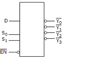
a) All are HIGH
b) All are LOW
c) All but Y0 are LOW
d) All but Y0 are HIGH
Explanation: In the given diagram, S0 and S1 are selection bits. So,
I/P S0 S1 O/P
D = 0 0 0 Y0
D = 0 0 1 Y1
D = 0 1 0 Y2
D = 0 1 1 Y3
Hence, inputs are S0 and S1 are Low means 0, so output is Y0 and rest all are HIGH.
4. The carry propagation can be expressed as ________
a) Cp = AB
b) Cp = A + B
c) All but Y0 are LOW
d) All but Y0 are HIGH
Explanation: This happens in parallel adders (where we try to add numbers in parallel via more than one adders). A carry propagation occurs when carry from one adder needs to be forwarded to other adder and that second adder is holding the computation (addition) because carry from first adder has not come yet. So, there is a slight delay for second adder and this is known as carry propagation
5. 3 bits full adder contains ________
a) 3 combinational inputs
b) 4 combinational inputs
c) 6 combinational inputs
d) 8 combinational inputs
Explanation: Full Adder is a combinational circuit with 3 input bits and 2 output bits CARRY and SUM. Three bits full adder requires 23 = 8 combinational circuits
6. What is a multiplexer?
a) It is a type of decoder which decodes several inputs and gives one output
b) A multiplexer is a device which converts many signals into one
c) It takes one input and results into many output
d) It is a type of encoder which decodes several inputs and gives one output
Explanation: A multiplexer (or MUX) is a device that selects one of several analog or digital input signals and forwards the selected input into a single line, depending on the active select lines.
7. Which combinational circuit is renowned for selecting a single input from multiple inputs & directing the binary information to output line?
a) Data Selector
b) Data distributor
c) Both data selector and data distributor
d) DeMultiplexer
Explanation: Data Selector is another name of Multiplexer. A multiplexer (or MUX) is a device that selects one of several analog or digital input signals and forwards the selected input into a single line, depending on the active select lines
8. It is possible for an enable or strobe input to undergo an expansion of two or more MUX ICs to the digital multiplexer with the proficiency of large number of ___________
a) Inputs
b) Outputs
c) Selection lines
d) Enable lines
Explanation: It is possible for an enable or strobe input to undergo an expansion of two or more MUX ICs to the digital multiplexer with the proficiency of large number of inputs
9. Which is the major functioning responsibility of the multiplexing combinational circuit?
a) Decoding the binary information
b) Generation of all minterms in an output function with OR-gate
c) Generation of selected path between multiple sources and a single destination
d) Encoding of binary information
Explanation: The major functioning responsibility of the multiplexing combinational circuit is generation of selected path between multiple sources and a single destination because it makes the circuit too flexible. A multiplexer (or MUX) is a device that selects one of several analog or digital input signals and forwards the selected input into a single line, depending on the active select lines.
10. What is the function of an enable input on a multiplexer chip?
a) To apply Vcc
b) To connect ground
c) To active the entire chip
d) To active one half of the chip
Explanation: Enable input is used to active the chip, when enable is high the chip works (ACTIVE), when enable is low the chip does not work (MEMORY). However, Enable can be Active-High or Active-Low, indicating it is active either when it is connected to VCC or GND respectively